Selenium nanomaterials enabled flexible and wearable electronics
Abstract
Selenium (Se), as an intriguing chalcogenide semiconductor, has traditionally been used for solar energy harvesting. The recent development of nanoscience and nanotechnology has enabled a myriad of Se nanomaterials with compelling structures and unique features. Compared with other chalcogens, Se nanomaterials possess anisotropic crystalline structure, intrinsic chirality, and high reactivity, as well as unique optical, electrical, photoconductive, and piezoelectrical properties. The integration of these Se nanomaterials with technologically important materials, such as conductors and semiconductors, over flexible, bendable, stretchable, and highly curved substrates offer a new generation of Se nanomaterial-based flexible and wearable electronics. In this mini review, we survey the recent scientific and technological breakthroughs in Se nanomaterials-enabled flexible and wearable electronics. We highlight the synthesis, fabrication, morphologies, structure, and properties (optical, electrical, optoelectrical, photovoltaic, and piezoelectric) of Se nanomaterials as well as their integration into innovative functional devices that deliver higher forms of applications across smart sensing, health care, and energy domains. We conclude with a critical analysis of existing challenges and opportunities that will trigger the continued progress of the field.
Keywords
INTRODUCTION
Flexible and wearable electronics capable of continuous monitoring of physiological signals[1-5], minimally invasive interrogation of neural circuitry[6-10], and performing diagnostic and therapeutic treatment[11-15] are offering unprecedented value to society and our everyday lives[16-20]. Functional materials that are responsive to stimuli (such as photons[21-25], stress[26-30], and chemicals[31-34]) are the core part of flexible and wearable electronics[35-37]. The incorporation of semiconducting materials with excellent electrical and optical properties into flexible and wearable electronics enables innovative smart devices and systems with powerful potential in personalized healthcare, precision medical surgery and large-area energy harvesting and storage[38-40]. Selenium (Se) is a trace element of group VI with a direct bandgap at room temperature[41]. Due to its unique band structure and crystal structure, Se, in its bulky form, shows attractive optical, electrical, electronic and piezoelectric properties opening up interesting applications in photodetection and solar energy harvesting[42-44]. Compared with typical semiconductors in electronic industry (such as silicon and germanium) that require sophisticated micro- and nanofabrication conditions, Se can be physically, thermally or chemically processed in simple, low-cost and robust manners, which makes its integration with flexible and wearable electronics straightforward, thereby enabling versatile devices and applications[45,46].
Thanks to the remarkable progress in nanofabrication and nanotechnology, bulky Se can be scaled down to tunable nanostructures ranging from zero-dimensional (0D) nanoparticles to two-dimensional (2D) nanosheets. Benefiting from the “nano-size” effect, Se nanomaterials exhibit distinct physical and chemical properties that cannot be found in their bulky counterparts, featuring improved mechanical, electrical, thermal, optical and piezoelectric performance[47-49]. Compared with other functional semiconducting nanomaterials such as Si nanowires, Ge nanowires and ZnSe nanowires employed in flexible electronics[50], Se nanomaterials show the distinctive advantage of processability. They can be easily integrated with traditional conductors and semiconductors over the flexible, bendable, stretchable, and highly curved substrates to fabricate innovative functional devices in the form factors of two-dimensional large-area films and patches as well as one-dimensional indefinitely long fibers as we elaborated in the section of “APPLICATIONS OF SELENIUM NANOMATERIALS IN FLEXIBLE AND WEARABLE ELECTRONICS”. This allows for the development of a new generation of Se nanomaterial-based flexible and wearable electronics. This mini review highlights the recent advances in Se nanomaterials enabled flexible and wearable electronics. We will first briefly review the typical morphologies and crystal structure of Se nanomaterials that directly determine their properties and subsequent applications. We will then present the synthesis and fabrication methodologies of Se nanostructures, namely the “bottom-up” and “top-down” strategies that have been widely exploited in the nanofabrication field. In the next section, we will discuss the physical properties of Se nanomaterials, focusing on optical, electrical, optoelectrical, photovoltaic, and piezoelectric behaviors that are of great importance for their functional applications in flexible and wearable electronics. Finally, we will discuss how Se nanomaterials can be integrated with substrates that are flexible, bendable, large-area and highly curved and how these innovative devices open up interesting opportunities in photosensing, mechanical deformation sensing, physiological sensing and energy storage. The review concludes with some key remaining challenges and perspectives that will be of value for future advances and breakthroughs in the field.
MORPHOLOGIES AND CRYSTAL STRUCTURES OF SELENIUM NANOMATERIALS
The morphologies, sizes and crystal structure of materials determine their properties and applications. We begin with a brief introduction to the morphologies and structure of Se nanomaterials.
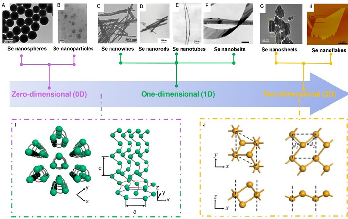
Generally, nanostructured Se can be categorized into zero-dimensional (0D), one-dimensional (1D), and two-dimensional (2D) form factors, as shown by the microscopic images in Figure 1 and Table 1. 0D Se nanomaterials include Se nanospheres and Se nanoparticles[51,52]. The synthesis method, surfactant or additive, reaction temperature, or reaction time influences their morphologies and properties. 1D Se nanomaterials have attracted lots of research interest recently because of their unique optical and electrical properties as well as potential employment in flexible electronics. A number of well-established techniques, mostly derived from “top-down” and “bottom-up” strategies, have been adopted to produce 1D nanostructures, including nanowires, nanorods, nanotubes, and nanobelts[53-56]. Compared with 1D metal nanomaterials, 1D Se nanomaterials show competitive advantages in terms of synthesis methodologies, structural and morphological tunability, and volumetric dispersion. Considerable efforts have been made to develop 2D Se nanomaterials since the emergence of Se nanoflakes in 2017[57]. 2D nanostructures have been demonstrated to be crucial and more suitable for device applications thanks to their high specific surface area, carrier capacity, energy storage ability, conversion efficiency, and environmental stability[58,59]. 2D Se nanomaterials offer a huge number of active sites on the surface for storing and transporting ions, thus acting as active electrode materials in energy storage systems[59].
Figure 1. (A) TEM image of Se nanosphere[51]; Copyright 2014, Elsevier. (B) TEM image of Se nanoparticles[52]; Copyright 2002, Wiley-VCH. (C) TEM image of Se nanowires[53]; Copyright 2015, Elsevier. (D) TEM image of Se nanorods[54]; Copyright 2004, Elsevier.
Summary of some representative synthesis methods, structures, properties, and applications of the Se nanomaterials
| Se morphology | Crystal structures | Synthesis methods | Precursors | Reaction conditions | Properties | Applications | Refs. |
| 0D nanoparticles | Hexagonal structure | Chemical reduction | Sodium selenite | Water, 2 ± 8 °C, 72 h | Anti hydroxyl radical property | Anti-oxidative stress drugs | [52] |
| 0D nanoparticles | Hexagonal structure | Solvent-thermal method | Selenous acid | Ethanol and distilled water, 150 °C, 24 h | Fluorescence property | Fluorescence sensors | [64] |
| 0D nanoparticles | Hexagonal structure | Laser-ablation method | Solide Se | Water, radiation wavelength of 1060 to 1070 nm, pulse repetition rate of 20 kHz, pulse duration of 80 ns | NA | Biological therapy | [65] |
| 0D nanoparticles | Hexagonal structure | Ball Milling and heating | Se bulk | Ball milling, 72 h, heating, | Electrical/Electrochemical properties | Li-Se batteries | [104] |
| 1D nanowires | Trigonal structure | Thermally-drawn assisted method | Se core | 260 °C, air atmosphere | Optoelectrical property | Fluorescence imaging fibers | [39] |
| 1D nanowires | Trigonal structure | Chemical reduction | SeO2 | Water, room temperature | Electrical property | Li-Se batteries | [53] |
| 1D nanorods | Hexagonal structure | Microwave-polyol method | SeO2 | 195 °C, 30 min, microwave heating | NA | NA | [54] |
| 1D nanotubes | Trigonal structure | Hydrothermal method | Sodium selenite | Water, 100 °C, 25 h | NA | NA | [55] |
| 1D nanobelts | Trigonal structure | Chemical reduction | Sodium selenite | Acid condition, | Optical property | Optical detector | [56] |
| 1D nanowires | Trigonal structure | Self-seeding solution-phase method | Selenious acid | Ice water | Optical/Photoconductivity property | Electronic, optical or mechanical nanodevices | [68] |
| 1D nanowires | Trigonal structure | Plasma-assisted selenization method | Se tank | 300 °C, plasma, heating | Optoelectrical property | Flexible photodetectors | [69] |
| 1D nanowire /nanotube | Trigonal structure | Thermally-drawn assisted method | Se rod | 260 °C, 30 min | Photoconductivity property | Optoelectronic detectors | [70] |
| 1D nanowires | Trigonal structure | Solvent-thermal method | SeO2 | Water and ethanol, 160 °C, 20 h | Piezoelectric property | Piezoelectric nanogenerators | [85] |
| 1D nanobelts | Trigonal structure | Thermal evaporation method | Se powder | 250 °C, 1 h, argon gas atmosphere | Electrical/ Photoconductivity property | Visible light photodetector | [94] |
| 2D nanosheets | Trigonal structure | Physical vapor deposition method | Se powder | 210 °C, 60 min argon atmosphere | Photoelectrical property | Phototransistors | [57] |
| 2D nanolayers | Hexagonal structure | Chemical vapor transport synthesis | Se powder | Liquid phase, hydrogen and argon gas atmosphere | NA | NA | [71] |
| 2D nanoflakes | Trigonal structure | Sonication liquid-phase exfoliation method | Bulk Se powder | IPA, 9 h, energy power of 600 W | Fluorescence property | Photoluminescence | [58] |
Se has six allotropic forms that can be classified as either crystalline or amorphous in the solid state based on its molecular structure[60,61]. There are five types of crystalline phases, including hexagonal Se with thermodynamic stability, a, b, c-monoclinic Se, rhombohedral Se, orthorhombic Se, and a and b-cubic Se. Non-crystalline allotropes of Se can be classified as amorphous and vitreous forms. The red and black amorphous Se is formed based on Se8 rings and Se8 chains, respectively, while vitreous Se is established on Se8 chains[62]. The chain arrangement greatly affects the electronic structure of Se[63]. For instance, monoclinic, amorphous, or another metastable Se is insulating. In contrast, trigonal Se is semiconducting. The atoms in trigonal Se are covalently bonded into spiral chains oriented along the c-axis, while the adjacent chains are weakly connected via van der Waals interactions and run along their radical directions, leading to a hexagonal structure [Figure 1I], which can facilitate electronic conduction[57]. The hexagonal structure exists in a wide range of 0D and 1D Se nanomaterials, enabling them to be promising semiconductors for optoelectronics and piezoelectronics. Because of the intrinsic anisotropy of the atomic structure, Se is prone to form 0D and 1D nanostructures, while 2D Se nanomaterials are relatively difficult to fabricate. It is reported that 2D Se nanomaterials have relatively complex structures based on crystal search computations. Besides the hexagonal and trigonal structure, two other stable structures including 1T-MoS2-like structure (T-Se) and square structure (S-Se) may exist [Figure 1J][63].
SYNTHESIS STRATEGIES AND FABRICATION TECHNIQUES OF SELENIUM NANOMATERIALS
The synthesis strategies and fabrication techniques greatly dictate the morphologies and structures of the resulting Se. So far, numerous protocols for synthesizing Se nanomaterials, such as chemical reduction, chemical vapor transfer synthesis, and thermally drawn-assisted synthesis, have been reported [Table 1]. The following section analyzes some representative synthesis and fabrication strategies of Se nanomaterials, including nanospheres, nanoparticles, nanotubes, nanowires, and nanosheets.
0D Se nanomaterial
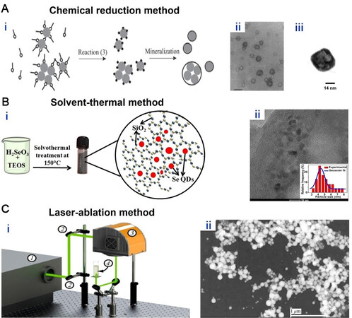
Due to the low cost, biocompatibility, and outstanding electrical properties, 0D Se nanomaterials have been brought into focus in chemical and material communities. Chemical reduction is one of the most common strategies for the synthesis of 0D Se. This approach involves reducing Se salts with various reducing chemicals. Se nanoparticles with a hollow structure synthesized by using A (Pr), sodium selenite, and mercaptothion as a template, Se sources, and reducing agents have been reported [Figure 2A][52]. TEM characterization revealed the hollow structures at the edges and centers. However, the obtained Se nanoparticles contain impurities, transferring these nanoscale materials is complicated, and breaking the serious aggregation remains challenging. All these issues restrict the practical application of these nanoparticles. The emergence of solvothermal synthesis successfully solves the problems, resulting in nanoparticles of high purity, uniform morphologies, and slight aggregation [Figure 2B][64]. Additionally, this method is facile to enable super-small nanoparticles. One example shown in Figure 2B (ii) shows nanoparticles with radii of 3-8 nm. In addition, laser ablation of solid bulky Se at the solid-liquid interface could also be harnessed to produce Se nanoparticles [Figure 2C][65]. With this “top-down” strategy, colloidal Se nanoparticles with sizes of below 100 nm are fabricated in pure water. Such Se nanoparticles are expected to be useful for biological applications. However, some issues that impede the practical application of 0D Se are also reported in these studies. For example, the collision and aggregation of Se nanoparticles frequently occurred, which easily led to serious surface oxidation and degradation. The research on oxidation and degradation will be at the center of the solvothermal synthesis of 0D Se nanomaterials.
Figure 2. (A) (i) Schematic illustration of the chemical reduction method[52]; (ii) TEM image of hollow sphere Se nanoparticles;
1D Se nanomaterials
1D Se nanomaterials such as nanowires, nanorods, nanotubes, and nanobelts have elicited significant interest because of their outstanding optical and electrical properties. Two strategies, namely the “top-down” and “bottom-up” approaches, have been generally employed for the synthesis of 1D formats. Specifically, the “top-down” strategy relies on selective removal of material from a solid bulky Se in a subtractive manner, while the “bottom-up” strategy utilizes individual atoms as the building blocks to realize structure assembling in an additive fashion[66,67].
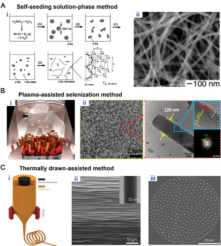
1D Se nanomaterials are commonly fabricated with the “bottom-up” approach because the atomic composition, size, and shape can be tailorable and controllable. This approach typically involves the decomposition of Se-based compound via chemical reactions either at room or an elevated temperature [Figure 3A]. The resulting nanowires are highly uniform, large-area and of high aspect ratio
Figure 3. (A) (i) Schematic illustration of self-seeding solution-phase method[68]; (ii) SEM image of Se nanowires; Copyright 2002, Wiley-VCH. (B) (i) Schematic of the plasma-assisted selenization process[69]; (ii) A top view SEM image of Se nanowires and a magnified TEM image of single Se nanowire with the lattice spacings of 0.351 nm of (110) and 0.502 nm of (001); Copyright 2018, American Chemical Society. (C) (i) Schematic illustration of thermally drawn-assisted method[70]; (ii) SEM image of Se nanowire arrays and inset is TEM image of a single nanowire with 32 nm thickness; (iii) Cross-sectional SEM micrograph of Se nanowires; Copyright 2011, Nature Publishing Group.
Although the bottom-up approach allows the massive production of Se nanowires at a low cost and in an efficient manner, the manipulation of the entangled nanowire mesh and their integration into devices remains challenging. Very recently, an impressive “top-down” route that exploits the thermal drawing approach has been developed to fabricate well-ordered, highly uniform Se nanowires and nanotubes
2D Se nanomaterials
2D nanomaterials have attracted exponentially increased academic attention since graphene was discovered. The unique physicochemical properties of 2D nanomaterials make them suitable for use in optoelectronics, electronics, energy storage, and catalysts. Due to Se’s intrinsic anisotropic atomic structure, the fabrication of 2D Se nanomaterials remains challenging as opposed to the 0D and 1D Se nanomaterials.
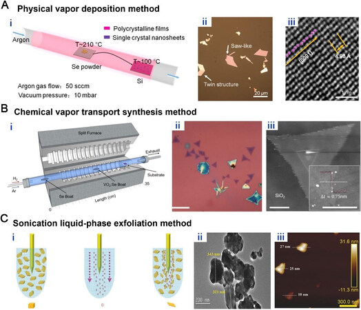
Physical vapor deposition (PVD), a thin-film coating process in which solid materials are vaporized under vacuum conditions and then deposited onto a substrate, has been considered as a promising technique for 2D Se nanomaterials fabrication. Se nanoflakes featured with thicknesses of 5 nm have been fabricated on a Si wafer substrate via depositing Se vapor generated from bulky Se powders [Figure 4A (i)][57]. The nanoflakes were irregularly shaped and zigzagged [Figure 4A (ii)]. Structural characterization reveals the helical atomic chains as well as lattice fringe spacing of typical trigonal structure [Figure 4A (iii)]. Chemical vapor transport (CVT) has also been emerging as one of the promising techniques for 2D Se nanomaterials fabrication[71]. CVT utilizes reversible chemical reactions to trigger crystal growth in different directions at different temperatures. The source materials are easy to obtain, and chemical reactions can be controlled. More importantly, the reactant composition can be easily tailored, thus enabling control over the characteristics of the targeted 2D Se nanomaterials. With this technique, Se nanosheets with typical trigonal crystals have been fabricated [Figure 4B (i)]. The thickness of the monolayer is 0.75 nm
Figure 4. (A) (i) Schematic diagram of the PVD method[57]; (ii) AFM height profile of a twin structure nanosheet; (iii) HAADF-STEM image of Se nanosheets; Copyright 2017, American Chemical Society. (B) (i) Schematic of the CVT method[71]; (ii) Optical microscope image of Se nanoflakes; (iii) AFM image of a Se nanoflake; Copyright 2018, © TÜRKİYE. (C) (i) Schematic demonstration of sonication liquid-phase exfoliation method[58]; (ii) TEM images of Se nanosheets; (iii) AFM images of Se nanosheets; Copyright 2017, Wiley-VCH.
However, stringent conditions such as ultrahigh vacuum and high temperature frustrate the large-scale production and potential applications of those 2D Se nanomaterials. Exploring more facile and green strategies and techniques is the mainstream direction for future development. Due to their strong in-plane chemical covalent bonds and weak out-of-plane van der Waals interactions, 2D Se nanomaterials can be readily fabricated by the well-established “top-down” methods, such as exfoliating from Se bulk materials in liquid phase. However, it is important to note that the processing temperature should be maintained at 0-10 ℃ in an ice bath, which can prevent the serious oxidation of Se nanostructures. Se nanosheets with ultrathin nanolayered structure have thus been fabricated in an isopropanol solution with probe sonication and centrifugation [Figure 4C (i)][58]. Under a low centrifugation speed, Se nanosheets showed average thicknesses of between 10 and 27 nm, whereas ultrathin features with average thicknesses of 3-6 nm were observed at high centrifugation speeds. TEM characterization revealed the lattice fringe spacings of 0.38, 0.22, and 0.29 nm, which correspond to the crystal plane spacings of (100), (110), and (101) planes
PROPERTIES OF SELENIUM NANOMATERIALS
As shown in Table 1, several unique properties of Se nanomaterials, including optical, optoelectronic and piezoelectric properties, and the morphologies and structure-properties relationship are briefly discussed in this section.
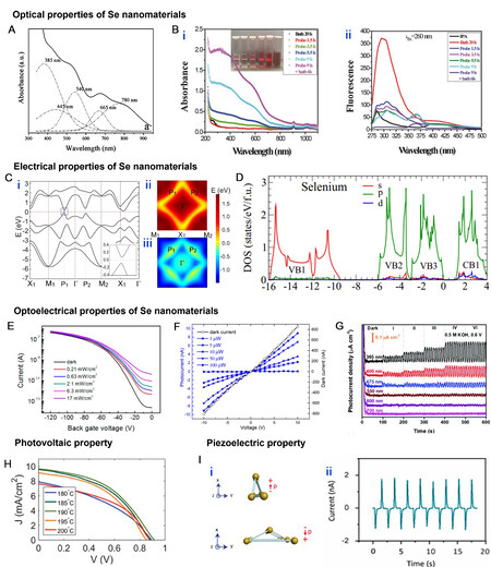
One of the attractive features is tunable and controllable optical properties caused by the quantum confinement effect. The optical properties of Se are of great importance for its photoconductive, photovoltaic and rectifying behaviors and, thus, its device application. Filippo et al. found that the UV-vis absorption spectrum of Se microtubes with nanoscale walls consisted of many bands that were typically observed in Se nanowires and some other distinct bands that could be attributed to the interchain interactions perpendicular to the c-axis [Figure 5A][72]. The optical properties of the nanostructured tubes are very different from those of the bulky Se powder source. Moreover, Xing et al. found that the optical properties of Se nanoflakes could be modulated through sonication treatments that affected the concentration of the formed Se nanoflakes, as demonstrated by the tunable optical absorbance versus sonication time [Figure 5B (i)][58]. Because of the fluorescence quenching effect and the equilibration of lateral sizes of Se nanoflakes, a new fluorescence emission peak appeared at 367 nm after 3.5 h sonication
Figure 5. (A) Room temperature UV-vis absorption spectrum[72]; Copyright 2010, American Chemical Society. (B) (i) UV-vis absorption spectrum; (ii) Fluorescence spectra with an excitation wavelength of 260 nm[58]; Copyright 2017, Wiley-VCH. (C) (i) Band structure; (ii) and (iii) Band contour for the bottom conduction band (upper panel) and the top valence band (lower panel) in the first Brillouin zone[61]; Copyright 2019; IOP Publishing. (D) Total and orbital-projected density of states (DOS) for Se[73]; Copyright 2019, American Physical Society. (E) Transfer curves of a Se nanosheet phototransistor measured under various laser irradiation powers at Vds = 3 V[57]; Copyright 2017, American Chemical Society. (F) Photocurrent as a function of laser illumination power measured from voltage of -10 V to 10 V[77]; Copyright 2017, Optical publishing group. (G) Photo response behaviors under lasers with various wavelengths and various laser power densities of dark and levels in 0.5 M KOH at a bias voltage of 0.6 V[78]; Copyright 2020, Royal society of chemistry. (H) J-V curves of Se-devices annealed at different specific temperatures[81]; Copyright 2019, Wiley-VCH.
Taking advantages of high photoconductivity, electrical anisotropy, and nonlinear optical properties, Se nanomaterials show great potential in optoelectrical applications[73-77]. Figure 5E shows the optoelectronic property of a phototransistor based on Se nanosheets[57]. The current-gate voltage curves show a gate tunability, where a photocurrent of up to 54 nA is generated even at a low illumination power of 0.21 mW cm-2. This result indicates an excellent photoresponsivity of Se nanosheets. Control over the grain size of Se can further increase the optoelectronic performance. For example, a laser-based annealing approach enabled a polycrystalline domain where the grain size was a few micrometers in the direction perpendicular to the electric field while the grain size was much smaller in the direction of illumination, which led to a super-sensitive photodetector with performance on par with some planar nanoscale devices [Figure 5F][77]. Besides 2D and 3D Se nanomaterials, 0D Se nanomaterials, such as Se quantum dots, also show excellent optoelectronic properties. As shown by Figure 5G, the photocurrent is detected in Se quantum dots under an applied bias voltage of 0.6 V[78]. Notably, the potential gradient generated within Se quantum dots promoted the separation of electrons and holes, thus enabling a higher photocurrent density (1.80 μA cm-2) than photodetectors based on Se nanosheets or Se nanowires.
Since its deployment in solar cells about 140 years ago, Se has been acting as a promising semiconducting material for the fabrication of photovoltaic devices[79,80]. Modulating crystalline structure can be an approach to improving solar cell efficiency. The relationship between solar cell performance and Se crystalline structure was investigated by Hadar et al.[81]. The presence of small crystal grains in Se’s structure, as shown in Figure 5H, contributed to the low short-circuit current density (Jsc), which could be explained by the low orientation order of the crystals. In addition, another efficient strategy to improve high solar cell efficiency is incorporating Se with other metal elements, such as germanium (Ge), copper (Cu), and indium (In)[82-84].
Piezoelectric properties are also discovered in Se nanomaterials. Se nanowires exhibit strong piezoelectric properties due to the anisotropic crystal structure of the trigonal phase [Figure 5I][85]. When longitudinal stress is applied along the x-axis, the Se atoms undergo internal displacement and the electronic charge is displaced against the Se cores, resulting in piezoelectric polarization parallel to the x-axis. When Se nanowires are stretched (compressed) vertically, piezoelectric polarization pointing upward (downward) is generated [Figure 5I (i)]. As a result, short-circuit current (Isc) is generated by compressing the Se nanowires along the alignment direction, showing a good perspective for piezoelectric nanogenerators [Figure 5I (ii)].
APPLICATIONS OF SELENIUM NANOMATERIALS IN FLEXIBLE AND WEARABLE ELECTRONICS
Several recent studies have demonstrated that Se nanomaterials represent an intriguing class of functional materials in flexible and wearable electronics because of their anisotropic structure, quantum confinement effects, large surface areas, and interesting optical, electrical, optoelectronic, electrochemical, photovoltaic, and piezoelectric properties. This section summarizes and discusses the fabrication and application of Se nanomaterials-based flexible or wearable electronics, including flexible and wearable sensors for photedetection, mechanical deformation sensing and physiological sensing, and flexible batteries.
Flexible and wearable sensors for biomedicine and healthcare
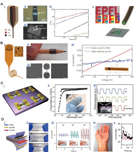
Selenium is an intriguing optoelectronic material, and its bulk form has been used for a myriad of optoelectronic applications in xerography, ultrasensitive imaging, chemical detection and photodiodes[86-89]. Selenium nanowires with a trigonal phase offer more appealing optoelectronic properties over their bulky form[90,91]. The integration of trigonal selenium nanowires into flexible devices is bringing novel opportunities for smart sensing, surgical tools and optogenetics[92,93]. The iterative thermal drawing discussed in the previous section enabled ultralong Se nanowire array to align along the fiber length. Interfacing the nanowires at the two extremities of the fiber with external electrodes formed a fiber-based photodetector that was sensitive to visible light[70]. However, the in-fiber selenium exhibited either an amorphous or a polycrystalline structure. The disorganized atomic arrangement and crystal defects like grain boundaries act as recombination centers for charge carriers, hindering the charge collection and reducing the photosensitivity and photoresponsivity. Yan et al. have recently devised a novel method that combines thermal drawing and sonochemical synthesis to create flexible fiber-based optoelectronic devices made of single-crystal semiconducting nanowires [Figure 6A][39]. The bulk in-fiber Se underwent a transformation into a dense array of nanowires through the manipulation of the anisotropy in the surface energy of the crystal’s crystal planes. The growth of single crystal nanowires from the amorphous bulk in 1-propanol resulted in the formation of in-fiber optoelectronic devices with built-in electrodes in intimate contact. These fiber devices showcased exceptional optical and optoelectronic performances, including high photoresponsivity and photosensitivity, low dark current, low noise-equivalent power, and ultrafast response speed, which rivaled many wafer-based devices. Notably, this innovative approach enabled high-throughput integration of nanowires into devices on an ultra-large scale, eliminating the need for intricate clean room contacting procedures. This was demonstrated through the growth of high-performance nanowire-based devices along the fiber length. The integration of multiple Se nanowire-based photodetectors and an optical fiber resulted in a hybrid fiber [Figure 6B][70]. The unique capability of this technology for fluorescent bioimaging based on the single multimodal fiber exhibiting simultaneous efficient optical guidance and excellent photodetection performance was demonstrated. The outstanding performance of the Se nanowires was analyzed to uncover the underlying mechanism. Ultrafast transient absorption spectroscopy, nanosecond flash photolysis, and time-resolved terahertz spectroscopy were used to study the charge carrier dynamics and mobility of Se nanowire meshes[11,31]. These noninvasive, contact-free methods uncovered a picosecond lifetime for free carriers and a microsecond lifetime for trapped carriers, both limited by trap-assisted recombination. Additionally, a high free carrier mobility of approximately 3.0 cm2 V-1 s-1 was discovered.
Figure 6. (A) (i) Schematic of multimaterials thermal drawing; (ii) Optical photograph of the cross section of the as-drawn fiber;
Due to their flexibility, small cross-section and high aspect ratio, fiber-shaped selenium nanowire optoelectronics are particularly useful for minimally invasive bioimaging, and remote and distributed photodetection. In addition to the fiber form factor, the selenium nanomaterials can also be integrated into large-area planar devices. Luo et al. reported fabrication of a thin film-based photodetector with full transparency and flexibility, in which the individual Se nanobelts were deposited on a flexible polyethylene terephthalate (PET) matrix [Figure 6C][94]. A number of characteristics were demonstrated to be impressive, including excellent transparency and flexibility, high light sensitivity, and stable response under various bending conditions.
By leveraging the piezoelectric property, selenium nanomaterials serve as excellent wearable sensors for mechanical deformation and physiological diagnosis. Wu et al. developed a Se nanowire-based piezoelectric nanogenerator (PENG) that consisted of PDMS layers, electrodes derived from Ag nanowires, and piezoelectric Se nanowires, as presented in Figure 6D[85]. Here, the PDMS layer serves two purposes: one is to act as the insulating layer between the Se and Ag nanowires, and the other is to encapsulate the Se and Ag nanowires to prevent oxidation and performance deterioration [Figure 6D (i)]. This device was flexible, stretchable, and robust enough to withstand mechanical deformation without breaking. Therefore, PENGs could be adhered to the skin of the human body to detect very faint deformations such as finger bending. The piezoelectric output voltage increases with the bending angle, allowing the finger movement to be recognized. Moreover, the nanogenerator could also be attached to a human wrist to detect the pulses of the radial artery in real time. Three distinct peaks are observed in the piezoelectric current output curve for the cardiac cycle. The P1, P2, and P3 represent the early systolic peak pressure, late systolic augmentation shoulder, and diastolic pulse waveform, respectively. These peaks can be valuable indicators to quantify the physiological information about the cardiovascular system of the wearer.
Flexible batteries
Recent studies have also demonstrated the huge potential of Se nanomaterials for high-performance electrodes in energy storage devices. Typical lithium-sulfur (Li-S) batteries show high theoretical specific capacities and energy densities. However, two major issues have hindered their practical application. First, sulfur is not a preferable electrode material because of its low electronic and ionic conductivity. Second, electrolyte-soluble polysulfide intermediate products are dissolvable in liquid electrolytes when a battery is working, leading to the significant shuttle effect and capacity loss[95-98].
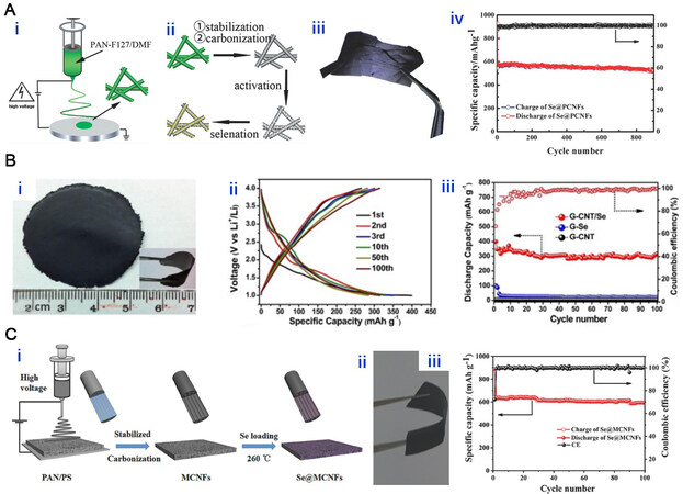
Se is an alternative to sulfur and has been used as a potential electrode material for Li-Se batteries[99-101]. However, bulky Se cathodes exhibit poor cycle performance and low Coulombic efficiency in comparison with S cathodes[102]. One strategy to overcome this issue is to incorporate Se into a 3D interconnected mesoporous carbon nanofibers (CNFs)[103]. This nanostructured Se/CNF enabled high-performance electrodes [Figure 7A]. The resulting Li-Se batteries can deliver a reversible capacity of 516 mAh g-1 after 900 cycles without any capacity loss at 0.5 A g-1.
Figure 7. (A) (i) and (ii) Schematic illustration of the synthesis process of the Se@PCNFs electrode; (iii) Photograph of free-standing and flexible Se@PCNFs electrode; (iv) Long-term cycling performance of Se@PCNFs electrode in Li-ion batteries at 0.5 A g-1 for 900 cycles[103]; Copyright 2015, Wiley-VCH. (B) (i) Digital photo of the flexible self-standing graphene-Se@CNT composite film;
Moreover, self-standing nanostructured graphene-Se@CNT film electrodes for Li-Se batteries have been synthesized[104]. The electrode displays high flexibility and bendability, as shown in Figure 7B. The flexible film cathode delivers a high reversible discharge capacity of 400 mAh g-1 that is slightly reduced to 315 mAh g-1, as well as a stable Coulombic efficiency above 96% even after 100 charging-discharging cycles. Nanostructured Se has also been integrated into Na-Se batteries for improved performance. For example, impregnating Se into microporous multichannel carbon nanofibers (MCNF) forms a self-standing cathode film in a Na-Se battery [Figure 7C] that exhibits an extraordinary discharge capacity (596 mA h g-1 at the 100th cycle at 0.1 A g-1), excellent rate capability (379 mA h g-1 at 2 A g-1), and long-time capacity durability over 300 charging-discharging cycles[105]. With more advances in performance, flexible batteries based on nanostructured Se might constitute a powerful platform for powering flexible and electronic devices and systems instead of using conventional heavy and rigid counterparts.
CONCLUSION AND OUTLOOK
Se nanomaterials are experiencing a flourishing research momentum. Advances in materials synthesis and fabrication, control over morphologies and structure, fundamental understanding of structure-properties relationship, and methodologies of devices integration offer a new class of Se nanomaterial-based flexible and wearable electronics, with wide-ranging applications in smart sensing, health care and energy. While the translation of nanoscale materials into macroscopic real devices is truly exciting, some challenges relevant to fundamental and applied science still exist.
Synthesis and fabrication: The fabrication of high-performance Se nanomaterial-based flexible and wearable electronic devices relies on the precise positioning and alignment of Se nanomaterials. Most existing approaches to Se nanomaterials synthesis are built upon solution-based processes that involve complex chemical reactions, producing Se nanomaterials with irregular positioning and agglomeration or entanglement. The fabrication of well-ordered, highly uniform Se nanomaterials remains a significant challenge. Moreover, the solution-based approaches, for the most part, exploit noxious raw materials such as Na2SeO3 and H2SeO3. Their inappropriate handling poses a significant threat to the environment. While solution-free methods such as PVD and CVT only process bulky Se, fulfilling the requirements of high temperature, high-vacuum environment, and highly purified gases demands high operation costs, which undermines the possibility of large-scale production. More controllable, effective, and eco-friendly synthesis and fabrication methods are heavily needed. The recent innovation in harnessing the multimaterial thermal drawing platform has demonstrated a unique and powerful platform for manufacturing periodic arrays of Se nanomaterials in an unprecedentedly green, sustainable and scalable manner[70,76,106-108]. The research along this direction has just begun and is expected to be an exciting paradigm for next-generation Se nanomaterial-based flexible and wearable electronics.
Structure-properties correlation: Se nanomaterials exhibit many intriguing optical, electrical, optoelectronic, photovoltaic, and piezoelectric properties. However, a deep understanding of the structure-properties correlation is still very limited. Harnessing sophisticated characterization techniques such as ultrafast transient absorption spectroscopy, nanosecond flash photolysis and time-resolved terahertz spectroscopy has paved a novel way toward this research direction[31]. This would allow us, on the one hand, to unravel the working principles of Se nanomaterial-based devices and, on the other hand, conversely tune the material structure to further improve performance.
Materials assembly and device integration: Most existing Se nanomaterials suffer from agglomeration or entanglement. Therefore, it requires a stringent post-synthesis process for materials alignment, assembly and device integration. Even though thermal drawing produces well-aligned and exquisitely controllable in-fiber nanomaterials, their monolithic integration with other functional materials such as electrodes for the fabrication of flexible and wearable electronic devices remains challenging. The difficulty is twofold: the co-drawing of Se with other functional materials is challenging because of their incompatible rheological properties; handling materials at the nanoscale is complicated. Nevertheless, an initial step with innovative advances in in-fiber nanowire self-assembly and simultaneous integration with built-in electrodes offers an appealing inspiration for us to further break through the roadblock[39]. More simpler and robust strategies for Se nanomaterials assembly and device integration are desirable for future real-world applications.
Se nanomaterial-based flexible and wearable electronics represent a class of technology with innovative potentials in smart sensing, health care and energy. With continued and concerted efforts in synthesis and fabrication, control over morphologies and structure, device assembly and integration, more advanced flexible and wearable electronics with more sophisticated functionalities and practical applications will emerge.
DECLARATIONS
Authors’ contributionsMade substantial contributions to the conception and design of the study: Dang C, Yan W
Writing-original draft preparation and review editing: Dang C, Liu M, Lin Z, Yan W
Availability of data and materialsNot applicable.
Financial support and sponsorshipYan W acknowledges the Nanyang Technological University (Start-up Grant 021850-00001: Yan W) and the National Natural Science Foundation of China (Grant No. 52202167).
Conflicts of interestAll authors declared that there are no conflicts of interest.
Ethical approval and consent to participateNot applicable.
Consent for publicationNot applicable.
Copyright© The Author(s) 2023.
REFERENCES
1. Yan W, Noel G, Loke G, et al. Single fibre enables acoustic fabrics via nanometre-scale vibrations. Nature 2022;603:616-23.
2. Yan W, Dong C, Xiang Y, et al. Thermally drawn advanced functional fibers: new frontier of flexible electronics. Mater Today 2020;35:168-94.
3. Zeng W, Shu L, Li Q, Chen S, Wang F, Tao XM. Fiber-based wearable electronics: a review of materials, fabrication, devices, and applications. Adv Mater 2014;26:5310-36.
4. Leber A, Dong C, Chandran R, Das Gupta T, Bartolomei N, Sorin F. Soft and stretchable liquid metal transmission lines as distributed probes of multimodal deformations. Nat Electron 2020;3:316-26.
6. Du M, Huang L, Zheng J, et al. Flexible fiber probe for efficient neural stimulation and detection. Adv Sci (Weinh) 2020;7:2001410.
7. Weng W, Yang J, Zhang Y, et al. A route toward smart system integration: from fiber design to device construction. Adv Mater 2020;32:e1902301.
9. Liu M, Lin Z, Wang X, et al. Focused rotary jet spinning: a novel fiber technology for heart biofabrication. Matter 2022;5:3576-9.
10. Jiang S, Patel DC, Kim J, et al. Spatially expandable fiber-based probes as a multifunctional deep brain interface. Nat Commun 2020;11:6115.
11. Xu B, Ma S, Xiang Y, et al. In-fiber structured particles and filament arrays from the perspective of fluid instabilities. Adv Fiber Mater 2020;2:1-12.
13. Wang H, Zhang Y, Liang X, Zhang Y. Smart fibers and textiles for personal health management. ACS Nano 2021;15:12497-508.
14. Zhang T, Li K, Zhang J, et al. High-performance, flexible, and ultralong crystalline thermoelectric fibers. Nano Energy 2017;41:35-42.
15. Martin-monier L, Gupta TD, Yan W, Lacour S, Sorin F. Nanoscale controlled oxidation of liquid metals for stretchable electronics and photonics. Adv Funct Mater 2021;31:2006711.
16. Pan S, Zhu M. Fiber electronics bring a new generation of acoustic fabrics. Adv Fiber Mater 2022;4:321-3.
17. Qian S, Liu M, Dou Y, Fink Y, Yan W. A ‘Moore’s law’ for fibers enables intelligent fabrics. Natl Sci Rev 2023;10:nwac202.
18. Loke G, Khudiyev T, Wang B, et al. Digital electronics in fibres enable fabric-based machine-learning inference. Nat Commun 2021;12:3317.
19. Kim J, Jia X. From space to battlefield: a new breed of multifunctional fiber sheets for extreme environments. Matter 2020;3:602-4.
20. Cao Y, Wu H, Allec SI, Wong BM, Nguyen DS, Wang C. A highly stretchy, transparent elastomer with the capability to automatically self-heal underwater. Adv Mater 2018;30:e1804602.
21. Hou C, Jia X, Wei L, et al. Crystalline silicon core fibres from aluminium core preforms. Nat Commun 2015;6:6248.
22. Wei L, Hou C, Levy E, et al. Optoelectronic fibers via selective amplification of in-fiber capillary instabilities. Adv Mater 2017;29:1603033.
23. Qu Y, Nguyen-Dang T, Page AG, et al. Superelastic multimaterial electronic and photonic fibers and devices via thermal drawing. Adv Mater 2018;30:e1707251.
24. Yan W, Burgos-caminal A, Das Gupta T, Moser J, Sorin F. Direct synthesis of selenium nanowire mesh on a solid substrate and insights into ultrafast photocarrier dynamics. J Phys Chem C 2018;122:25134-41.
25. Chin AL, Jiang S, Jang E, et al. Implantable optical fibers for immunotherapeutics delivery and tumor impedance measurement. Nat Commun 2021;12:5138.
26. Dong C, Leber A, Das Gupta T, et al. High-efficiency super-elastic liquid metal based triboelectric fibers and textiles. Nat Commun 2020;11:3537.
27. Cao Y, Morrissey TG, Acome E, et al. A Transparent, self-healing, highly stretchable ionic conductor. Adv Mater 2017;29:1605099.
28. Yan W, Richard I, Kurtuldu G, et al. Structured nanoscale metallic glass fibres with extreme aspect ratios. Nat Nanotechnol 2020;15:875-82.
29. Nguyen-dang T, de Luca AC, Yan W, et al. Controlled sub-micrometer hierarchical textures engineered in polymeric fibers and microchannels via thermal drawing. Adv Funct Mater 2017;27:1605935.
30. Zhang Y, Li X, Kim J, et al. Thermally drawn stretchable electrical and optical fiber sensors for multimodal extreme deformation sensing. Adv Optical Mater 2021;9:2001815.
31. Jiang S, Song J, Zhang Y, et al. Nano-optoelectrodes integrated with flexible multifunctional fiber probes by high-throughput scalable fabrication. ACS Appl Mater Interfaces 2021;13:9156-65.
32. Das Gupta T, Martin-Monier L, Yan W, et al. Self-assembly of nanostructured glass metasurfaces via templated fluid instabilities. Nat Nanotechnol 2019;14:320-7.
33. Kim J, Zhao Y, Yang S, et al. Laser machined fiber-based microprobe: application in microscale electroporation. Adv Fiber Mater 2022;4:859-72.
34. Dong C, Page AG, Yan W, Nguyen-dang T, Sorin F. Microstructured multimaterial fibers for microfluidic sensing. Adv Mater Technol 2019;4:1900417.
35. Grena B, Alayrac JB, Levy E, Stolyarov AM, Joannopoulos JD, Fink Y. Thermally-drawn fibers with spatially-selective porous domains. Nat Commun 2017;8:364.
36. Sun H, Xie S, Li Y, et al. Large-area supercapacitor textiles with novel hierarchical conducting structures. Adv Mater 2016;28:8431-8.
37. Khudiyev T, Lee JT, Cox JR, et al. 100 m long thermally drawn supercapacitor fibers with applications to 3D printing and textiles. Adv Mater 2020;32:e2004971.
38. Zhang J, Zhang T, Zhang H, et al. Single-crystal snse thermoelectric fibers via laser-induced directional crystallization: from 1d fibers to multidimensional fabrics. Adv Mater 2020;32:e2002702.
39. Yan W, Qu Y, Gupta TD, et al. Semiconducting nanowire-based optoelectronic fibers. Adv Mater 2017;29:1700681.
40. Hou C, Jia X, Wei L, et al. Direct atomic-level observation and chemical analysis of ZnSe synthesized by in situ high-throughput reactive fiber drawing. Nano Lett 2013;13:975-9.
41. Zhang H, li L, Zheng D, et al. Broadband photodetector based on vapor-deposited selenium self-supporting films. Ceramics International 2022;48:27750-7.
43. Hu K, Chen H, Jiang M, Teng F, Zheng L, Fang X. Broadband photoresponse enhancement of a high-performance
44. Kumar M, Dubey A, Adhikari N, Venkatesan S, Qiao Q. Strategic review of secondary phases, defects and defect-complexes in kesterite CZTS-Se solar cells. Energy Environ Sci 2015;8:3134-59.
45. Wang S, Liu X, Zhou P. The road for 2D semiconductors in the silicon age. Adv Mater 2022;34:e2106886.
46. Kang SK, Park G, Kim K, et al. Dissolution chemistry and biocompatibility of silicon- and germanium-based semiconductors for transient electronics. ACS Appl Mater Interfaces 2015;7:9297-305.
47. Khalid A, Tran PA, Norello R, Simpson DA, O’Connor AJ, Tomljenovic-Hanic S. Intrinsic fluorescence of selenium nanoparticles for cellular imaging applications. Nanoscale 2016;8:3376.
48. Ramírez-montes L, López-pérez W, González-hernández R, Pinilla C. Large thermoelectric figure of merit in hexagonal phase of 2D selenium and tellurium. Int J Quantum Chem 2020:120.
49. Qin JK, Zhou F, Wang J, Chen J, et al. Anisotropic signal processing with trigonal selenium nanosheet synaptic transistors. ACS Nano 2020;14:10018-26.
50. Huang W, Wang M, Hu L, Wang C, Xie Z, Zhang H. Recent advances in semiconducting monoelemental selenium nanostructures for device applications. Adv Funct Mater 2020;30:2003301.
51. Kumar A, Sevonkaev I, Goia DV. Synthesis of selenium particles with various morphologies. J Colloid Interf Sci 2014;416:119-123.
52. Gao X, Zhang J, Zhang L. Hollow sphere selenium nanoparticles: their
53. Zhang J, Xu Y, Fan L, Zhu Y, Liang J, Qian Y. Graphene-encapsulated selenium/polyaniline core-shell nanowires with enhanced electrochemical performance for Li-Se batteries. Nano Energy 2015;13:592-600.
54. Zhu Y, Hu X. Preparation of powders of selenium nanorods and nanowires by microwave-polyol method. Mater Lett 2004;58:1234-6.
55. Xi G, Xiong K, Zhao Q, Zhang R, Zhang H, Qian Y. Nucleation-dissolution-recrystallization: a new growth mechanism for
56. Ma Y, Qi L, Shen W, Ma J. Selective synthesis of single-crystalline selenium nanobelts and nanowires in micellar solutions of nonionic surfactants. Langmuir 2005;21:6161-4.
57. Qin J, Qiu G, Jian J, et al. Controlled growth of a large-size 2D selenium nanosheet and its electronic and optoelectronic applications. ACS Nano 2017;11:10222-9.
58. Xing C, Xie Z, Liang Z, et al. 2D Nonlayered selenium nanosheets: facile synthesis, photoluminescence, and ultrafast photonics. Adv Optical Mater 2017;5:1700884.
59. Shi Z, Zhang H, Khan K, Cao R, Xu K, Zhang H. Two-dimensional selenium and its composites for device applications. Nano Res 2022;15:104-22.
60. Liu C, Hu T, Wu Y B, et al. 2D selenium allotropes from first principles and swarm intelligence. J Phys Condens Matter 2019;31:235702.
61. Xian L, Pérez Paz A, Bianco E, Ajayan PM, Rubio A. Square selenene and tellurene: novel group VI elemental 2D materials with nontrivial topological properties. 2D Mater 2017;4:041003.
62. Degtyareva O, Gregoryanz E, Somayazulu M, Mao H, Hemley RJ. Crystal structure of the superconducting phases of S and Se. Phys Rev B 2005;71:214104.
64. Anupama K, Paul T, Mary KAA. Solid-state fluorescent selenium quantum dots by a solvothermal assisted sol-gel route for curcumin sensing. ACS Omega 2021;6:21525-33.
65. Ayyyzhy KO, Voronov VV, Gudkov SV, Rakov II, Simakin AV, Shafeev GA. Laser fabrication and fragmentation of selenium nanoparticles in aqueous media. Phys Wave Phen 2019;27:113-8.
66. Salazar-alvarez G, Muhammed M, Zagorodni AA. Novel flow injection synthesis of iron oxide nanoparticles with narrow size distribution. Chem Eng Sci 2006;61:4625-33.
67. Basak S, Chen D, Biswas P. Electrospray of ionic precursor solutions to synthesize iron oxide nanoparticles: modified scaling law. Chem Eng Sci 2007;62:1263-8.
68. Gates B, Mayers B, Cattle B, Xia Y. Synthesis and characterization of uniform nanowires of trigonal selenium. Adv Funct Mater 2002;12:219.
69. Chen YZ, You YT, Chen PJ, et al. Environmentally and mechanically stable selenium 1D/2D hybrid structures for broad-range photoresponse from ultraviolet to infrared wavelengths. ACS Appl Mater Interfaces 2018;10:35477-86.
70. Yaman M, Khudiyev T, Ozgur E, et al. Arrays of indefinitely long uniform nanowires and nanotubes. Nat Mater 2011;10:494-501.
71. Kasirga TS. Chemical vapor transport synthesis of a selenium-based two-dimensional material. Turk J Phys 2018:42.
72. Filippo E, Manno D, Serra A. Characterization and growth mechanism of selenium microtubes synthesized by a vapor phase deposition route. Crystal Growth & Design 2010;10:4890-7.
73. Cheng M, Wu S, Zhu Z, Guo G. Large second-harmonic generation and linear electro-optic effect in trigonal selenium and tellurium. Phys Rev B 2019:100.
74. Jun SW, Jeon S, Kwon J, Lee J, Kim C, Hong SW. Full-color laser displays based on optical second-harmonic generation from the thin film arrays of selenium nanowires. ACS Photonics 2022;9:368-77.
75. Gumennik A, Stolyarov AM, Schell BR, et al. All-in-fiber chemical sensing. Adv Mater 2012;24:6005-9.
76. Deng DS, Orf ND, Abouraddy AF, et al. In-fiber semiconductor filament arrays. Nano Lett 2008;8:4265-9.
77. Yan W, Nguyen-dang T, Cayron C, et al. Microstructure tailoring of selenium-core multimaterial optoelectronic fibers. Opt Mater Express 2017;7:1388.
78. Jiang X, Huang W, Wang R, et al. Photocarrier relaxation pathways in selenium quantum dots and their application in UV-Vis photodetection. Nanoscale 2020;12:11232-41.
79. Shin D, Zhu T, Huang X, Gunawan O, Blum V, Mitzi DB. Earth-abundant chalcogenide photovoltaic devices with over 5% efficiency based on a Cu2 BaSn(S,Se)4 absorber. Adv Mater 2017;29:1606945.
80. Jayswal NK, Rijal S, Subedi B, et al. Optical properties of thin film Sb2Se3 and identification of its electronic losses in photovoltaic devices. Solar Energy 2021;228:38-44.
81. Hadar I, Song T, Ke W, Kanatzidis MG. Modern processing and insights on selenium solar cells: the world’s first photovoltaic device. Adv Energy Mater 2019;9:1802766.
82. Liu SC, Dai CM, Min Y, et al. An antibonding valence band maximum enables defect-tolerant and stable GeSe photovoltaics. Nat Commun 2021;12:670.
83. Seo Y, Lee B, Jo Y, et al. Facile microwave-assisted synthesis of multiphase CuInSe2 nanoparticles and role of secondary cuse phase on photovoltaic device performance. J Phys Chem C 2013;117:9529-36.
84. Ulaganathan RK, Yadav K, Sankar R, Chou FC, Chen Y. Hybrid InSe nanosheets and MoS2 quantum dots for high-performance broadband photodetectors and photovoltaic cells. Adv Mater Interfaces 2019;6:1801336.
85. Wu M, Wang Y, Gao S, et al. Solution-synthesized chiral piezoelectric selenium nanowires for wearable self-powered human-integrated monitoring. Nano Energy 2019;56:693-9.
86. Harkin JM, Dong A, Chesters G. Elevation of selenium levels in air by xerography. Nature 1976;259:204-5.
87. Zhu B, Wu L, Wang Y, et al. A highly selective and ultrasensitive ratiometric far-red fluorescent probe for imaging endogenous peroxynitrite in living cells. Sensor Actuat B-Chem 2018;259:797-802.
88. Manjare ST, Kim Y, Churchill DG. Selenium- and tellurium-containing fluorescent molecular probes for the detection of biologically important analytes. Acc Chem Res 2014;47:2985-98.
89. Triet Ho LT, Mukherjee A, Vasileska D, et al. Modeling dark current conduction mechanisms and mitigation techniques in vertically stacked amorphous selenium-based photodetectors. ACS Appl Electron Mater 2021;3:3538-46.
90. Liao ZM, Hou C, Liu LP, Yu DP. Temperature dependence of photoelectrical properties of single selenium nanowires. Nanoscale Res Lett 2010;5:926-9.
91. Luo LB, Jie JS, Chen ZH, et al. Photoconductive properties of selenium nanowire photodetectors. J Nanosci Nanotechnol 2009;9:6292-8.
92. Akiyama N. A sensor array based on trigonal-selenium nanowires for the detection of gas mixtures. Sensor Actuat B-Chem 2016;223:131-7.
93. Yan W, Page A, Nguyen-Dang T, et al. Advanced multimaterial electronic and optoelectronic fibers and textiles. Adv Mater 2019;31:e1802348.
94. Luo L, Yang X, Liang F, et al. Transparent and flexible selenium nanobelt-based visible light photodetector. CrystEngComm 2012;14:1942.
95. Ji L, Rao M, Zheng H, et al. Graphene oxide as a sulfur immobilizer in high performance lithium/sulfur cells. J Am Chem Soc 2011;133:18522-5.
96. Bruce PG, Freunberger SA, Hardwick LJ, Tarascon JM. Li-O2 and Li-S batteries with high energy storage. Nat Mater 2011;11:19-29.
97. Luo C, Xu Y, Zhu Y, et al. Selenium@mesoporous carbon composite with superior lithium and sodium storage capacity. ACS Nano 2013;7:8003-10.
98. Guo J, Xu Y, Wang C. Sulfur-impregnated disordered carbon nanotubes cathode for lithium-sulfur batteries. Nano Lett 2011;11:4288-94.
99. Abouimrane A, Dambournet D, Chapman KW, Chupas PJ, Weng W, Amine K. A new class of lithium and sodium rechargeable batteries based on selenium and selenium-sulfur as a positive electrode. J Am Chem Soc 2012;134:4505-8.
100. Liu L, Hou Y, Wu X, et al. Nanoporous selenium as a cathode material for rechargeable lithium-selenium batteries. Chem Commun (Camb) 2013;49:11515-7.
101. Yang CP, Xin S, Yin YX, Ye H, Zhang J, Guo YG. An advanced selenium-carbon cathode for rechargeable lithium-selenium batteries. Angew Chem Int Ed Engl 2013;52:8363-7.
102. Zhang Z, Zhang Z, Zhang K, Yang X, Li Q. Improvement of electrochemical performance of rechargeable lithium-selenium batteries by inserting a free-standing carbon interlayer. RSC Adv 2014;4:15489-92.
103. Zeng L, Zeng W, Jiang Y, et al. A flexible porous carbon nanofibers-selenium cathode with superior electrochemical performance for both Li-Se and Na-Se batteries. Adv Energy Mater 2015;5:1401377.
104. Han K, Liu Z, Ye H, Dai F. Flexible self-standing graphene-Se@CNT composite film as a binder-free cathode for rechargeable Li-Se batteries. J Power Sources 2014;263:85-9.
105. Yuan B, Sun X, Zeng L, Yu Y, Wang Q. A Freestanding and long-life sodium-selenium cathode by encapsulation of selenium into microporous multichannel carbon nanofibers. Small 2018;14:1703252.
106. Marion JS, Gupta N, Cheung H, Monir K, Anikeeva P, Fink Y. Thermally drawn highly conductive fibers with controlled elasticity. Adv Mater 2022;34:e2201081.
107. Deng DS, Nave JC, Liang X, Johnson SG, Fink Y. Exploration of in-fiber nanostructures from capillary instability. Opt Express 2011;19:16273-90.
Cite This Article
Export citation file: BibTeX | RIS
OAE Style
Dang C, Liu M, Lin Z, Yan W. Selenium nanomaterials enabled flexible and wearable electronics. Chem Synth 2023;3:14. http://dx.doi.org/10.20517/cs.2022.33
AMA Style
Dang C, Liu M, Lin Z, Yan W. Selenium nanomaterials enabled flexible and wearable electronics. Chemical Synthesis. 2023; 3(2): 14. http://dx.doi.org/10.20517/cs.2022.33
Chicago/Turabian Style
Dang, Chao, Mingyang Liu, Zhiwei Lin, Wei Yan. 2023. "Selenium nanomaterials enabled flexible and wearable electronics" Chemical Synthesis. 3, no.2: 14. http://dx.doi.org/10.20517/cs.2022.33
ACS Style
Dang, C.; Liu M.; Lin Z.; Yan W. Selenium nanomaterials enabled flexible and wearable electronics. Chem. Synth. 2023, 3, 14. http://dx.doi.org/10.20517/cs.2022.33
About This Article
Special Issue
Copyright
Author Biographies



Data & Comments
Data
 Cite This Article 16 clicks







Comments
Comments must be written in English. Spam, offensive content, impersonation, and private information will not be permitted. If any comment is reported and identified as inappropriate content by OAE staff, the comment will be removed without notice. If you have any queries or need any help, please contact us at support@oaepublish.com.